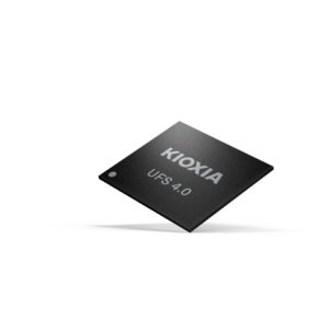
QLC UFS NAND from Kioxia
by David Manners · Electronics Weekly.comKioxia is mass production of a QLC UFS flash memory.
The 512GB QLC UFS chip has sequential read speeds of up to 4,200 MB/s and sequential write speeds of up to 3,200 MB/s, taking full advantage of the UFS 4.0 interface speed
Key Features include:
Supports High Speed Link Startup Sequence (HS-LSS) features: With conventional UFS, Link

Startup (M-PHY and UniPro initialisation sequence) between device and host is performed at low-speed PWM-G1 (3~9Mbps), but with HS-LSS, it can be performed at a faster HS-G1 Rate A (1,248 Mbps). This is expected to reduce the time for Link Startup by approximately 70% compared to the conventional method.
- Enhances security: By utilizing Advanced RPMB (Replay Protected Memory Block) for improved read and write access to security data, such as user credentials on RPMB area, and RPMB Purge to ensure discarded data may be sanitised securely and rapidly.
- Supports Extended Initiator ID (Ext-IID): Intended to be used with Multi Circular Queue (MCQ) at the UFS 4.0 host controller for improved random performance.
The new QLC UFS Ver. 4.0 device integrates the company’s innovative BiCS FLASH 3D flash memory and a controller in a JEDEC standard package. UFS 4.0 incorporates MIPI M-PHY 5.0 and UniPro 2.0 and supports maximum theoretical interface speeds of up to 23.2Gbps per lane or 46.4 Gbps per device. UFS 4.0 is backward compatible with UFS 3.1.